
GameBoy on KR260: the retrogaming journey
Introduction
Get ready for a fascinating journey into the world of gaming nostalgia! In this tutorial, we'll explore how to bring the beloved GameBoy architecture to life on AMD's FPGA KR260. We'll walk you through the process step by step, making it easy for you to embark on this exciting adventure. And the best part? We're sharing the open-source code on GitHub, so you can join in the fun and experience the magic of retro gaming firsthand!
The GameBoy architecture
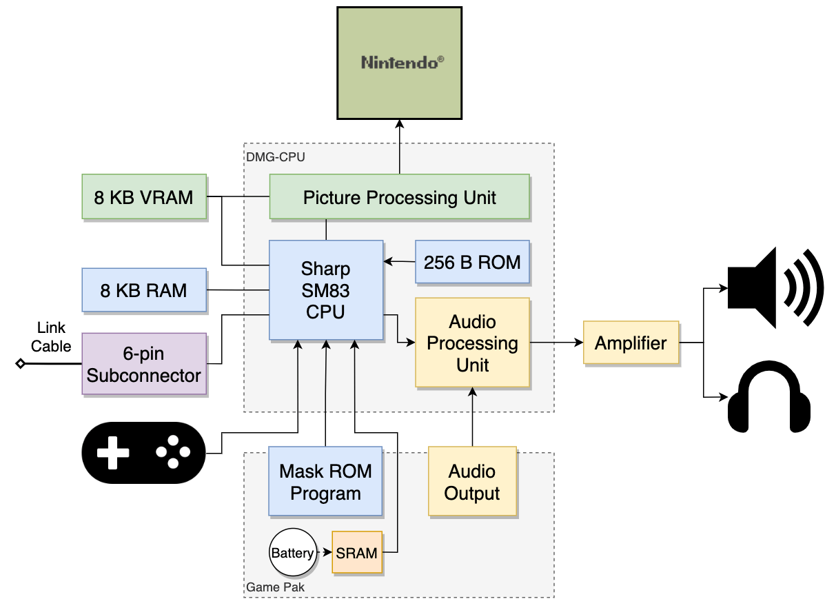
The GameBoy architecture, a legendary handheld console, is a marvel of simplicity and ingenuity. At its core lies an 8-bit Sharp LR35902 processor, running at a modest 4.19 MHz. This processor handles the execution of game instructions, while also managing the system's memory and I/O operations.
Then, the GameBoy features an 8 KB internal RAM, for storing program data and variables during gameplay. Additionally, there is 8 KB of Video RAM (VRAM) dedicated to rendering graphics on the 160x144 pixel LCD screen.
Also, the sound is a crucial part of the GameBoy experience, and its architecture includes a 4-channel audio system. This system generates waveforms and handles mixing to produce a range of catchy tunes and sound effects.
A custom 8-bit GPU implements the GameBoy's graphics capabilities as the Picture Processing Unit (PPU). It supports a palette of 56 colors and can display sprites and backgrounds with various scrolling and tile mapping techniques.
To enable game cartridges, the GameBoy incorporates a cartridge connector for external memory. Cartridges can contain additional ROM or RAM, allowing for expanded game data and save functionality.
The GameBoy audio
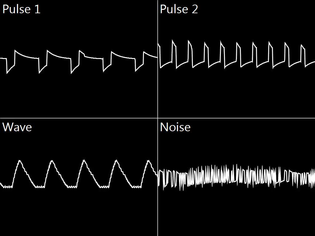
The GameBoy boasts a charmingly simplistic yet versatile audio system, consisting of four distinct channels. Each channel serves a specific purpose, contributing to the immersive auditory experience of games.
- Square Wave Channel 1 (Tone 1 & Sweep): This channel generates square wave tones with variable frequencies and adjustable duty cycles. It also features a frequency sweep functionality that produces a sliding effect, adding dynamic sound variations.
- Square Wave Channel 2 (Tone 2): Similar to Channel 1, this channel produces square wave tones with independent frequency and duty cycle control. It allows for creating harmonies and layered melodies.
- Waveform Channel (Wave): The Wave channel utilizes a programmable waveform table, enabling the playback of sampled sound effects or more complex waveforms. It offers a broader range of tones and sound textures.
- Noise Channel: As the name suggests, this channel generates noise-like sounds. It can mimic percussion instruments, white noise, or various sound effects. It provides an element of randomness and adds depth to the overall audio experience.
Finally, these four channels can be individually configured and mixed together to create a rich soundscape for GameBoy games. By combining their capabilities, game developers were able to compose catchy tunes, atmospheric soundtracks, and memorable sound effects, all within the limitations of GameBoy's hardware.
The VerilogBoy project
There is a remarkable repository called VerilogBoy that houses a highly accurate and generic implementation of the GameBoy architecture specifically tailored for AMD's FPGA devices. This repository provides a comprehensive Verilog codebase that faithfully emulates the functionalities and behavior of the original GameBoy hardware.
In particular, VerilogBoy offers meticulous and detailed implementation, ensuring precise compatibility and reliable performance on AMD FPGAs. It serves as a valuable resource for FPGA enthusiasts, retro gaming enthusiasts, and developers looking to explore the world of GameBoy emulation on FPGA platforms.
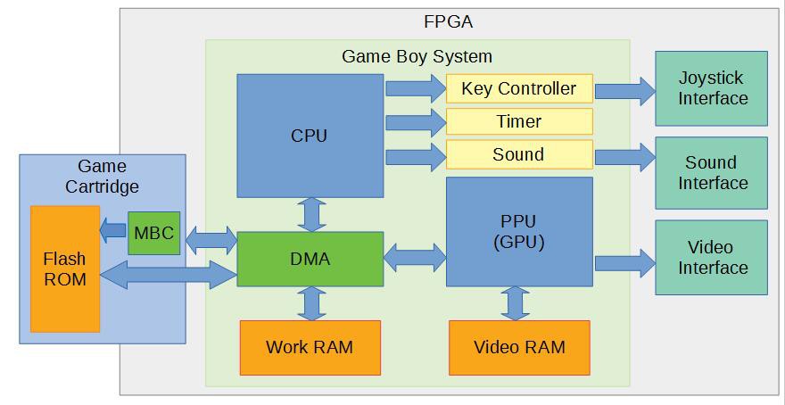
This repository contains those components:
- the CPU implementation with the controller input;
- a bootable and configurable ROM;
- the cartridge paging (MBC5);
- the PPU (Pixel Processing Unit);
- the sound unit.
So, let's start to port it!
The GameBoy implementation
We can choose 2 modalities of implementation: the block design flow or the Verilog Top Flow. We prefer the Verilog Top Flow because the design is very complex and has a lot of different IPs. The full code is here.
So, let's analyze the Top module.
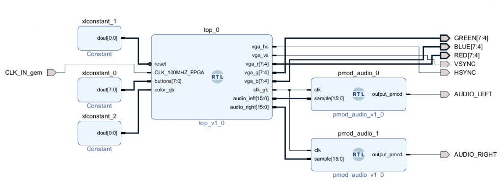
- Inputs:
reset: A wire representing the reset signal for the system.CLK_100MHZ_FPGA: The input clock signal from the FPGA operating at 100 MHz (for KR260, we have used the carrier card oscillator with 25MHz and we will setup later to the Clocking Wizard).buttons: An 8-bit wire representing the input from the GameBoy buttons.color_gb: A wire indicating whether the GameBoy should output color or grayscale.
- Outputs:
vga_hs,vga_vs: Wires representing the horizontal and vertical sync signals for VGA output.vga_r,vga_g,vga_b: 4-bit wires representing the red, green, and blue color components for VGA output.clk_gb: The output clock signal for synchronizing GameBoy operations.audio_left,audio_right: 16-bit wires for audio output, representing the left and right audio channels.
The code includes instantiations of different modules, such as the PLL (Phase-Locked Loop, in our case a Clocking Wizard IP) for generating different clock signals, the Boy module responsible for emulating the GameBoy system, the MBC5 module for managing the memory bank controller operations, and the VGA mixer module for generating VGA output signals.
It also includes connections to other modules, such as the cartridge for reading ROM and RAM data, the single-port RAM for managing cartridge RAM operations, and the vga_mixer module for combining GameBoy image data with VGA signals.
The audio output module
An important mention is the audio output, driven with the "pmod_audio" module that works as a sigma-delta modulator (PWM DAC).
This module called pmod_audio, implements a simple audio output functionality for a specific sampling rate using a counter and a PWM (Pulse Width Modulation) signal. Let's understand the different components and their connections:
- Inputs:
clk: The input clock signal with a frequency of 21.477 MHz.sample: A 16-bit wire representing the audio sample input. The sampling rate for this module is 42 kHz.
- Outputs:
output_pmod: The PWM signal output for the Pmod audio module.
- Internal Signals:
counter: A 9-bit register used as a counter to control the timing of the audio output.audio_latched: A 16-bit register used to store the latched audio sample.aud_pwm: A 1-bit register representing the PWM output signal.
The module uses an always block triggered by the positive edge of the clk signal. Inside the always block, the following operations take place:
- If the
countervalue is 0, the currentsamplevalue is latched into theaudio_latchedregister. - Depending on the value of
counterandaudio_latched, theaud_pwmregister is set accordingly. Whencounteris less than 1 or the value formed by concatenatingcounterwith 7 zeros is less thanaudio_latched(in a 512 sample range),aud_pwmis set to 1, otherwise, to 0. - The
countervalue is incremented by 1.
Finally, the aud_pwm register is assigned to the output_pmod wire, representing the PWM output of the module.
Overall, this module allows for audio output by generating a PWM signal based on the input audio samples and the specified sampling rate.
Load new Cartridge
In Vivado, it is possible to load new GameBoy cartridges into the design, not limited to the one provided in the repository. To accomplish this, it is necessary to convert a dump file of an original cartridge into a COE file. Let's explain what a COE file is in the context of Vivado.
In Vivado, a COE (Coefficient) file is a text-based file format used to describe the contents of a memory initialization file (MIF) for initializing memory blocks within a digital design. The COE file specifies the initial values to be loaded into memory locations, such as ROM or RAM.
The COE file format consists of lines of data representing memory locations and their corresponding values. Each line typically includes the memory address and the data value associated with it. The file may also contain additional information such as the memory width, radix, or data organization.
When working with GameBoy cartridges, the original cartridge dump file is converted into a COE file format compatible with Vivado. This conversion process involves parsing the data from the cartridge dump and formatting it into the appropriate COE file structure.
Once the cartridge dump is converted into a COE file, it can be used as an input in Vivado's memory initialization process. Vivado will then utilize the COE file to initialize the memory blocks in the FPGA design with the contents of the GameBoy cartridge, allowing for the loading and execution of custom GameBoy games or applications.
By converting the cartridge dump into a COE file and integrating it into the Vivado design flow, users can extend the functionality of the GameBoy FPGA implementation and explore a wider range of games and software on their GameBoy emulator.
Utility tools
In the repository, specifically in the "tools" folder, there is a Python script called "bin2hex_coe.py." This script serves the purpose of converting a cartridge dump file into both a hexadecimal file and a COE file.
The "bin2hex_coe.py" script takes as input a binary file that represents the cartridge dump. It then performs the following conversions:
- Hexadecimal Conversion: The script reads the binary file and converts its contents into a hexadecimal format.
- COE Conversion: Additionally, the script generates a COE file from the binary data. It follows the COE file format structure, which includes specifying memory addresses and their associated data values. The script parses the binary file and formats the data accordingly to generate the COE file.
By running the "bin2hex_coe.py" script on the cartridge dump file, users can obtain both the hexadecimal file and the COE file. The hexadecimal file provides a human-readable representation of the cartridge dump in hexadecimal format. The COE file, on the other hand, allows for easy integration with Vivado or other tools that require a memory initialization file in the COE format.
This script simplifies the process of converting cartridge dump files into the necessary formats for further use in FPGA designs, enabling users to conveniently work with custom cartridges and expand the capabilities of the GameBoy FPGA implementation.
Load the COE file into the design
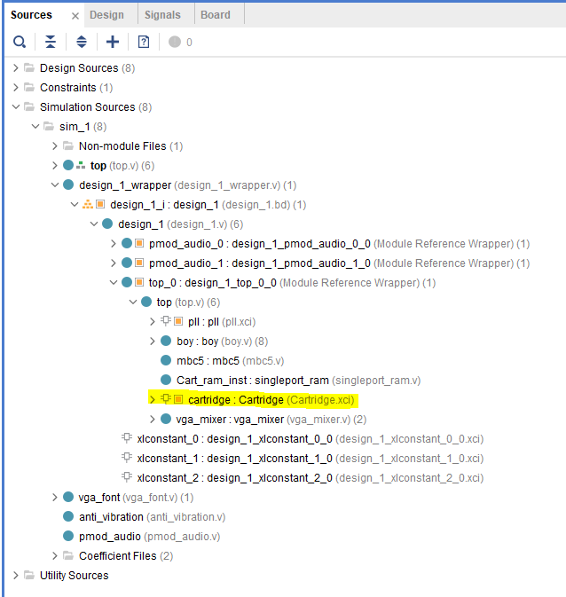
In the Vivado design, the project's IP Inspector provides a convenient way to manage and configure various IP cores used in the design. Search the IP "Cartridge," which represents a ROM memory component. In this case, we will utilize this IP core to load the COE file.
To load the COE file into the Cartridge IP core, you can follow these steps:
- Open the Vivado project and navigate to the IP Inspector panel, which typically resides on the left-hand side of the Vivado interface.
- Locate the "Cartridge" IP core within the IP Inspector.
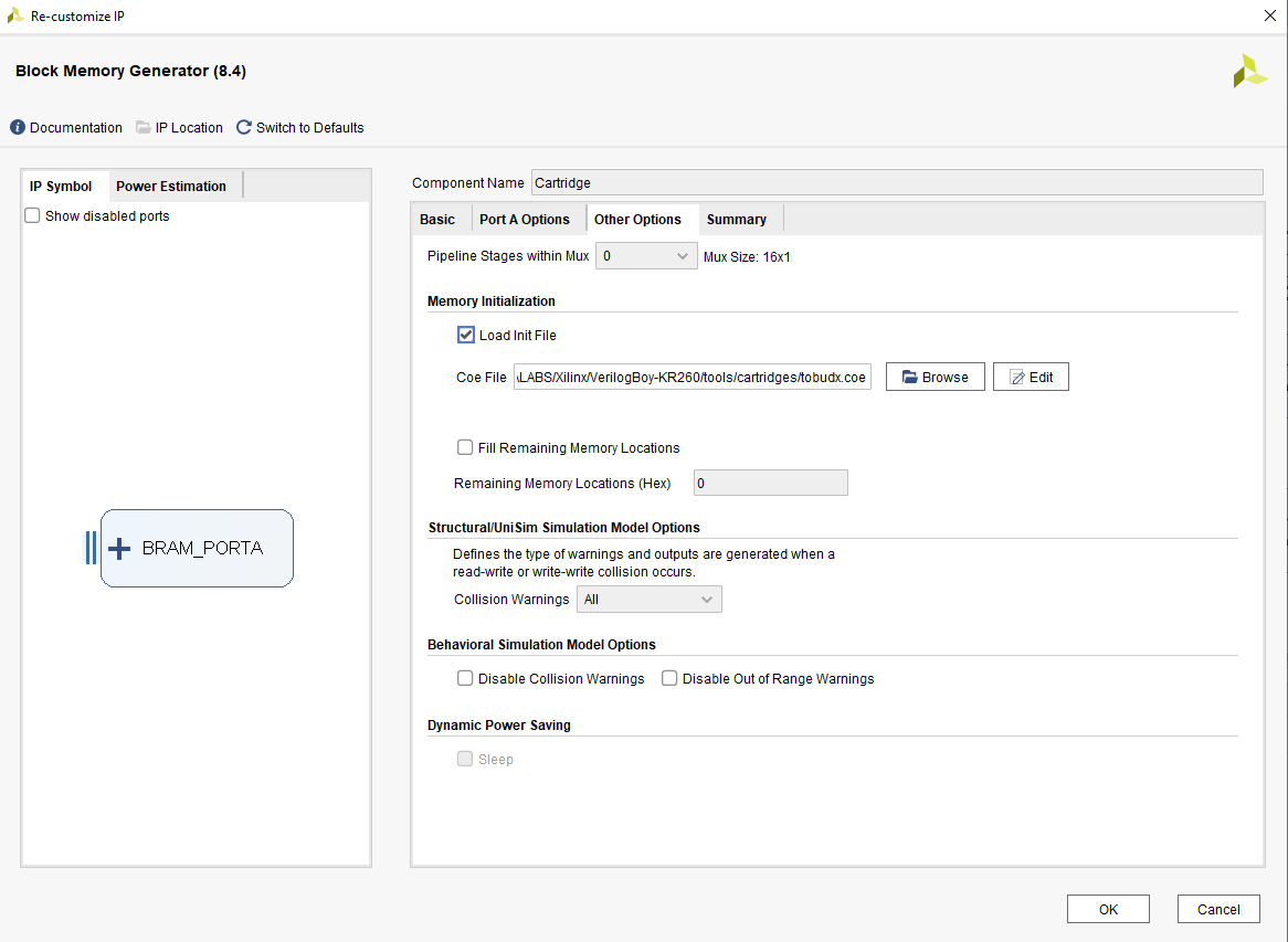
- Right-click on the "Cartridge" IP core and select the "Re-customize IP" option. This will open a configuration dialog box specific to the Cartridge IP core.
- Within the configuration dialog box, find the option related to memory initialization or memory content.
- In the memory initialization or content option, specify the path to the COE file that you want to load into the Cartridge IP core.
- Once the COE file is specified, save the configuration changes and close the configuration dialog box.
- Finally, re-implement or regenerate the design in Vivado to apply the changes made to the Cartridge IP core.
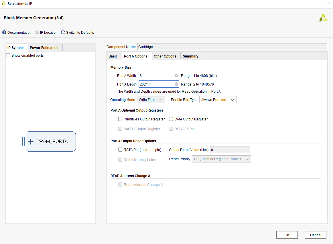
Port depth size of the ROM
You should set the size of the memory in the Cartridge IP core based on the number of lines present in the hex file. Each line corresponds to the size of the ROM memory.
To properly set the memory size, you can follow these additional steps:
- After specifying the COE file in the memory initialization or content option of the Cartridge IP core configuration dialog box, open the COE file using a text editor.
- Count the number of lines in the COE file. Each line represents a memory location and its associated data value.
- Once you have the number of lines, adjust the memory size configuration in the Cartridge IP core accordingly. This ensures that the ROM memory size matches the number of lines in the COE file.
- Save the changes to the Cartridge IP core configuration and proceed to re-implement or regenerate the design in Vivado.
By setting the memory size correctly, you align the Cartridge IP core's memory capacity with the contents of the COE file. This ensures that the ROM memory can accommodate the entire data from the cartridge, allowing for accurate emulation and execution of the GameBoy program within the FPGA design.

[…] GameBoy on KR260: the retrogaming journey […]