
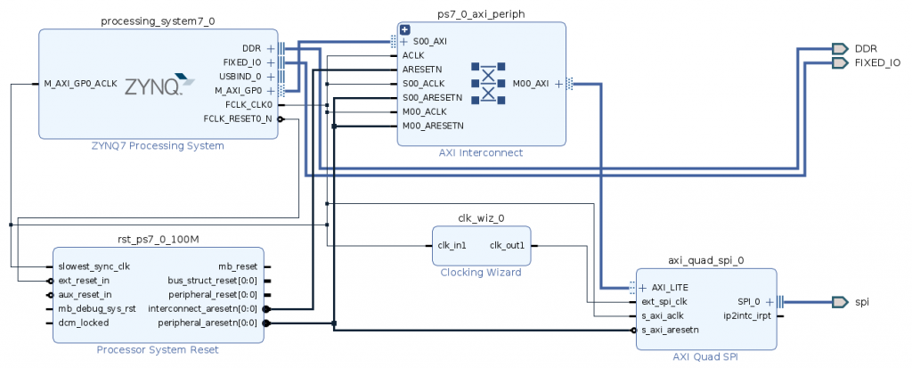
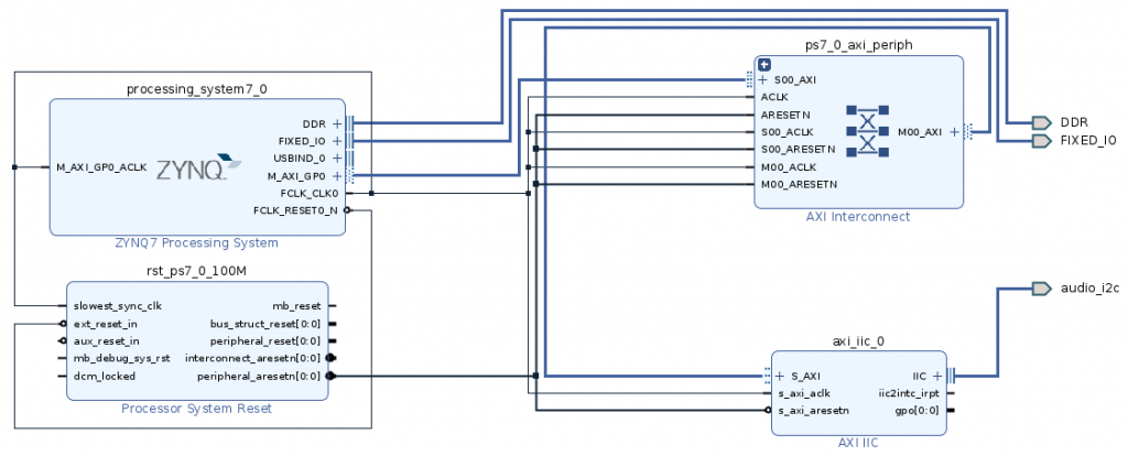
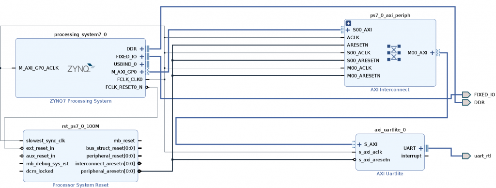
SPI, I2C, UART on PYNQ: a PL approach
Let’s start using as example of the PYNQ Z2 schematic. You can find the schematics in this link:
https://dpoauwgwqsy2x.cloudfront.net/Download/TUL_PYNQ_Schematic_R12.pdf
So, let’s check the schematics:
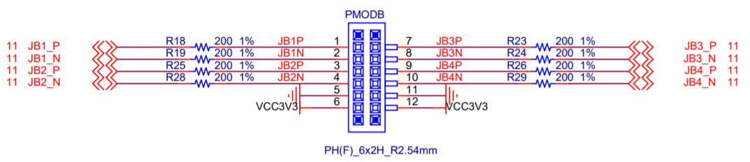
The pins 5 and 11 are Ground connection, while 6 and 12 are VCC 3.3V connection. Remember that you will need to connect the Ground pin to your external board, in order to share the ground for both PYNQ Z2 board and the other board. You also need to know that the VCC reference is 3.3V, so if the other device works with a different voltage, the communication will be unstable or impossible to understand!
The pins 1, 2, 3, 4, 7, 8, 9, 10 are free, so you can use it freely. So, take the pin 1 and 2 for Rx and Tx, you see that pins 1 and 2 have labels JB1_P and JB1_N, so these are the names of the link between PMODB and FPGA. Now, we need to find in the schematics where are JB1_P and JB1_N, in order to obtain the real name of the FPGA pins connected to these links.

Ok, fortunately you can use in the most of the schematics the CTRL+F command (find text), but always is a bit struggling!
So, let’s check the links for the JB1_P and JB1_N:
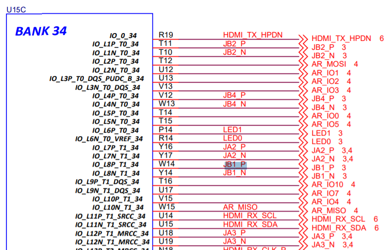
You see that there is a connection between JB1_P and W14 pin of the FPGA and between JB1_N and Y14 pin, so we did it! We will use them on Vivado in order to create the constraint file.

[…] If you need to go into details about the hardware design, please read this article […]
[…] create pinout interfaces with the right constraints according to the PMOD pinout, see this article if you need to know how) […]
[…] Peripheral tutorial article […]
[…] For all the details on how to get to this design and how to manage the various constraints, we recommend the following article: spi-i2c-uart-on-pynq-a-pl-approach. […]
Hi, after building the bitstream, how to deploy the kernel onto the target board?
Hi! You need to use this command:
ol = Overlay(“your bitstream name”)
You can use the full code described here: https://github.com/MakarenaLabs/Common-PL-Devices-on-PYNQ
Can i use this to implement multiplier on PL and Send the result to the PS?
[…] don’t know what we’re talking about and want more details? click_here to see our article on how to create a UART communication on […]
[…] LINK TO THE ARTICLE : https://www.makarenalabs.com/spi-i2c-uart-on-pynq-a-pl-approach/ […]
[…] you need to know more precisely how to control PYNQ, GPIO, and Microblaze, take a look at the GPIO article and Microblaze […]
hi! i’m a new user of pynq z2. i have pulled a tissue in the github page which you mentioned above. Beg you will see this.
I’m try to connect bluetooth model HM10 to the pynq z2 via PMOD B with the exact block design as described in the UART, and after syntetesis and validation I’m generating bit stream and fogram the device via the vivado 2018.1, and run the python code that showing hare : https://github.com/MakarenaLabs/Common-PL-Devices-on-PYNQ but the response from the module is: ERROR,
For the purpose of testing I connected the module to Arduino and the response for AT command is ok,
steps already done: baud rate = 9600, verify connection (rx> tx, tx>rx, vcc=3.3v frome the pynq, gnd from the pynq) ,what do i missing here? if you have any idea I would love to hear
can i use this to implement multiplier on PL and send the result to PS using UART?
Can i use this to implement multiplier on PL and Send the result to the PS?